Semiconductor RF chips and their vacuum coating processes
Editorial:2025-11-14
The core function of the radio frequency chip is to handle the transmission and reception of radio signals, enabling efficient data transmission and connection of wireless communication devices . It is widely used in fields such as mobile phones, the Internet of Things, automotive radars, base stations, and defense systems. The radio frequency Chip (RF Chip) serves as the "signal translator" and "transmission bridge" of wireless communication systems. Its core mission is to achieve the transmission and reception, modulation and demodulation, and signal optimization of high-frequency electrical signals. It converts the digital signals processed by the baseband chip into RF signals that can be transmitted through antennas, while simultaneously receiving external RF signals and restoring them to digital signals. From mobile phone calls to satellite communications, from Internet of Things transmission to car radars, the signal transmission in all wireless connection scenarios relies on the precise operation of radio frequency chips.
Key characteristics and performance of RF chips: High-frequency processing capability : covering the 300kHz to 300GHz frequency band, compatible with different protocols. Youdaoplaceholder0 Low noise and high integration : noise figure <1.5dB, supporting multi-band integration (such as 2G to 5G). Youdaoplaceholder0 Environmental adaptability: It adopts a wide temperature range design (-40℃ to 125℃) and anti-interference packaging (such as RF QFN) to ensure stability in complex electromagnetic environments.
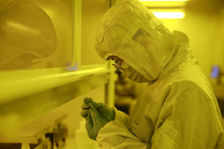
The substrate (mostly silicon-based, GaAs or GaN wafers) needs to undergo multi-stage cleaning and surface activation to ensure there is no interference from impurities. Firstly, ultrasonic cleaning technology is adopted. In an environment ranging from 50°C to 80°C, solvents and deionized water are alternately used to remove surface grease and particulate contaminants. Subsequently, the surface is activated through plasma treatment to optimize the roughness and enhance the adhesion of the film layer. In some scenarios, chemical corrosion is required to further improve the interface bonding performance. After cleaning, it needs to be dried in a 190°C oven to remove moisture, and then precisely fixed to the coating fixture through a fully automatic mounting machine to avoid secondary contamination.
A combined system of molecular pumps and ion pumps is adopted for vacuuming to achieve a high vacuum or ultra-high vacuum state of 10⁻³ to 10⁻⁷Pa in the coating chamber. The stable control of vacuum degree is of vital importance. It can effectively reduce the interference of gas molecules on the transmission of evaporated particles, prevent the formation of pores and impurity inclusions in the film layer, and directly affect the loss characteristics of radio frequency signal transmission.
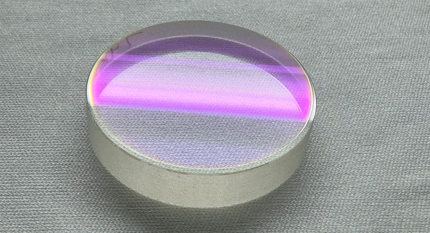
According to the function of the film layer, the corresponding target material is selected and pre-treated. Commonly used target materials for metal electrodes include gold, molybdenum, titanium, etc., while for piezoelectric layers, scandium-doped aluminum nitride target materials are mostly adopted. At the same time, set key process parameters: The substrate temperature needs to take into account both crystallization quality and thermal sensitivity, and is usually controlled at 200 to 500°C. Reactive sputtering requires precise adjustment of the flow rate ratio of argon to oxygen/nitrogen to control the composition ratio of oxide and nitride film layers. The deposition rate is monitored in real time by a quartz crystal microbalance to ensure that the thickness deviation of the film layer is within the nanometer range.
The core function of the radio frequency chip is to handle the transmission and reception of radio signals, enabling efficient data transmission and connection of wireless communication devices . It is widely used in fields such as mobile phones, the Internet of Things, automotive radars, base stations, and defense systems. The radio frequency Chip (RF Chip) serves as the "signal translator" and "transmission bridge" of wireless communication systems. Its core mission is to achieve the transmission and reception, modulation and demodulation, and signal optimization of high-frequency electrical signals. It converts the digital signals processed by the baseband chip into RF signals that can be transmitted through antennas, while simultaneously receiving external RF signals and restoring them to digital signals. From mobile phone calls to satellite communications, from Internet of Things transmission to car radars, the signal transmission in all wireless connection scenarios relies on the precise operation of radio frequency chips.
Key characteristics and performance of RF chips: High-frequency processing capability : covering the 300kHz to 300GHz frequency band, compatible with different protocols. Youdaoplaceholder0 Low noise and high integration : noise figure <1.5dB, supporting multi-band integration (such as 2G to 5G). Youdaoplaceholder0 Environmental adaptability: It adopts a wide temperature range design (-40℃ to 125℃) and anti-interference packaging (such as RF QFN) to ensure stability in complex electromagnetic environments.
The substrate (mostly silicon-based, GaAs or GaN wafers) needs to undergo multi-stage cleaning and surface activation to ensure there is no interference from impurities. Firstly, ultrasonic cleaning technology is adopted. In an environment ranging from 50°C to 80°C, solvents and deionized water are alternately used to remove surface grease and particulate contaminants. Subsequently, the surface is activated through plasma treatment to optimize the roughness and enhance the adhesion of the film layer. In some scenarios, chemical corrosion is required to further improve the interface bonding performance. After cleaning, it needs to be dried in a 190°C oven to remove moisture, and then precisely fixed to the coating fixture through a fully automatic mounting machine to avoid secondary contamination.
A combined system of molecular pumps and ion pumps is adopted for vacuuming to achieve a high vacuum or ultra-high vacuum state of 10⁻³ to 10⁻⁷Pa in the coating chamber. The stable control of vacuum degree is of vital importance. It can effectively reduce the interference of gas molecules on the transmission of evaporated particles, prevent the formation of pores and impurity inclusions in the film layer, and directly affect the loss characteristics of radio frequency signal transmission.
According to the function of the film layer, the corresponding target material is selected and pre-treated. Commonly used target materials for metal electrodes include gold, molybdenum, titanium, etc., while for piezoelectric layers, scandium-doped aluminum nitride target materials are mostly adopted. At the same time, set key process parameters: The substrate temperature needs to take into account both crystallization quality and thermal sensitivity, and is usually controlled at 200 to 500°C. Reactive sputtering requires precise adjustment of the flow rate ratio of argon to oxygen/nitrogen to control the composition ratio of oxide and nitride film layers. The deposition rate is monitored in real time by a quartz crystal microbalance to ensure that the thickness deviation of the film layer is within the nanometer range.

Ningbo Top Score Vacuum Technology Co., Ltd is a specialist manufacturer/exporter of vacuum products.


Copyright © 2024 Ningbo Top Score Vacuum Technology Co.,Ltd.